The origin of VLSI or Very Large Scale Integration dates back to the 1970s. This revolutionary design helped to combine thousands of transistors into a single chip and thus creating integrated circuits. Because of the VLSI technology we have now the modern day computers and laptop, which occupy much less space and perform even better than the primarily invented computers. The products designed by VLSI technology makes the product cheap and also makes it run faster and consume less power. VLSI technology has made electronic goods affordable.
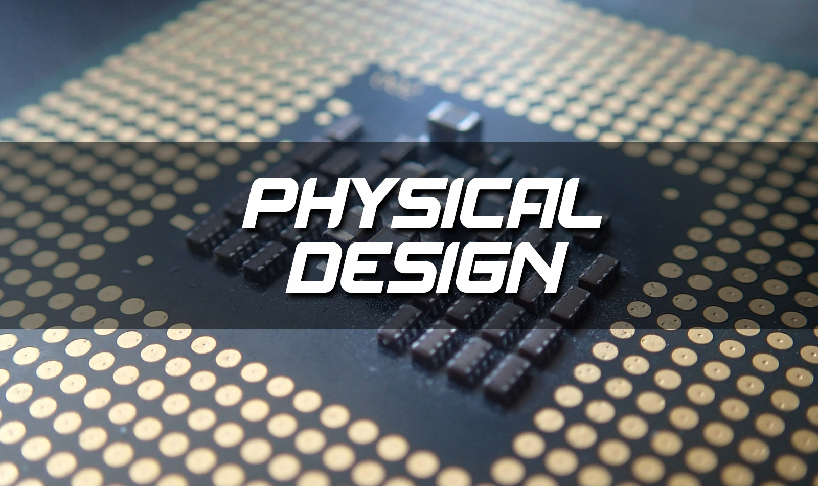
These days, the VLSI mainly consists of Front End Design and Back End Design. The front end design comprises of design verification, digital design including HDL, design for testability and other different kinds of verification techniques. The back end design however consists of CMOS library design and the characterization that it has. It further consists the fault simulation and physical design.
If you are an engineer who has a keen interest in the electronic engineering field then you opt for VLSI training. Once you complete your VLSI Bangalore training from a good and reputed institute, you are likely to get a decent job. However, to enter the VLSI field, you need to have a high CGPA and if you want to opt for foreign universities then your GRE score needs to be high as well.
In today’s world of technology, the VLSI market is blooming. VLSI devices are found almost everywhere around us now. VLSI chips are put to use in cell phones, cars, cameras, household appliances, medical devices and in carious other places. Because of this high market reach, this sector is now offering a lot of jobs where one can build a strong future. In order to secure a job in the VLSI field, one needs to have hands on experience in the field of engineering, electronic circuit deigns along with hardware description languages and most importantly, the skills to have knowledge about the know-how of the concepts of practice of VLSI.
There is a constant need of designing integrated circuits because of the advancements in the field of technology. Since, everyday use worthy products like the smart phones are being updated and brought in the market with new features and shorter running cycle, the needs for talented VLSI consultants grow larger by the day.
If you happen to be someone who is interested in the VLSI field but do not know where to look while searching for the right VLSI coaching centres in Bangalore then you should get in touch with some institute that is reliable. Such institute will offer one of the best trainings in the VLSI field and should also have a strong base of faculty members who are very strong in their own field. Moreover, the faculties appointed in your selected institute should actually be professionals from the semiconductor technology field and thus they should be experienced with hands on experience. You should also make sure that your selected institute also offers different courses on design of VLSI on a very scheduled manner. Finally you should check the website of the institute for all the necessary details.
In recent years, demand for chip-driven products has increased significantly in consumer electronics, medical electronics, communications, aerospace, computers, and many other fields. Given this tremendous market demand, more and more chip design companies are establishing units in India and seeking Indian talent. Also, many of India’s leading IT companies have made extensive efforts to design application-specific integrated circuits (ASICs).
The rapid expansion of the design and manufacturing market (domestic and international) has increased the demand for trained professionals to improve the technical workforce of the VLSI domain. That why student look for best VLSI training institutes in Bangalore.
VLSI training process
The best VLSI training institutes in Bangalore provides students with complete knowledge of the flow of ASIC and FPGA design. VLSI training process is designed with the current requirements of the current semiconductor industry in mind. VLSI training institutes focused to train the students in front-end design and ASIC verification practices. A good Institute’s goal is not only to have VLSI students acquire all the skills they need in VLSI, find jobs in the forefront companies but also be successful in the industry based on ASIC and FPGA design.